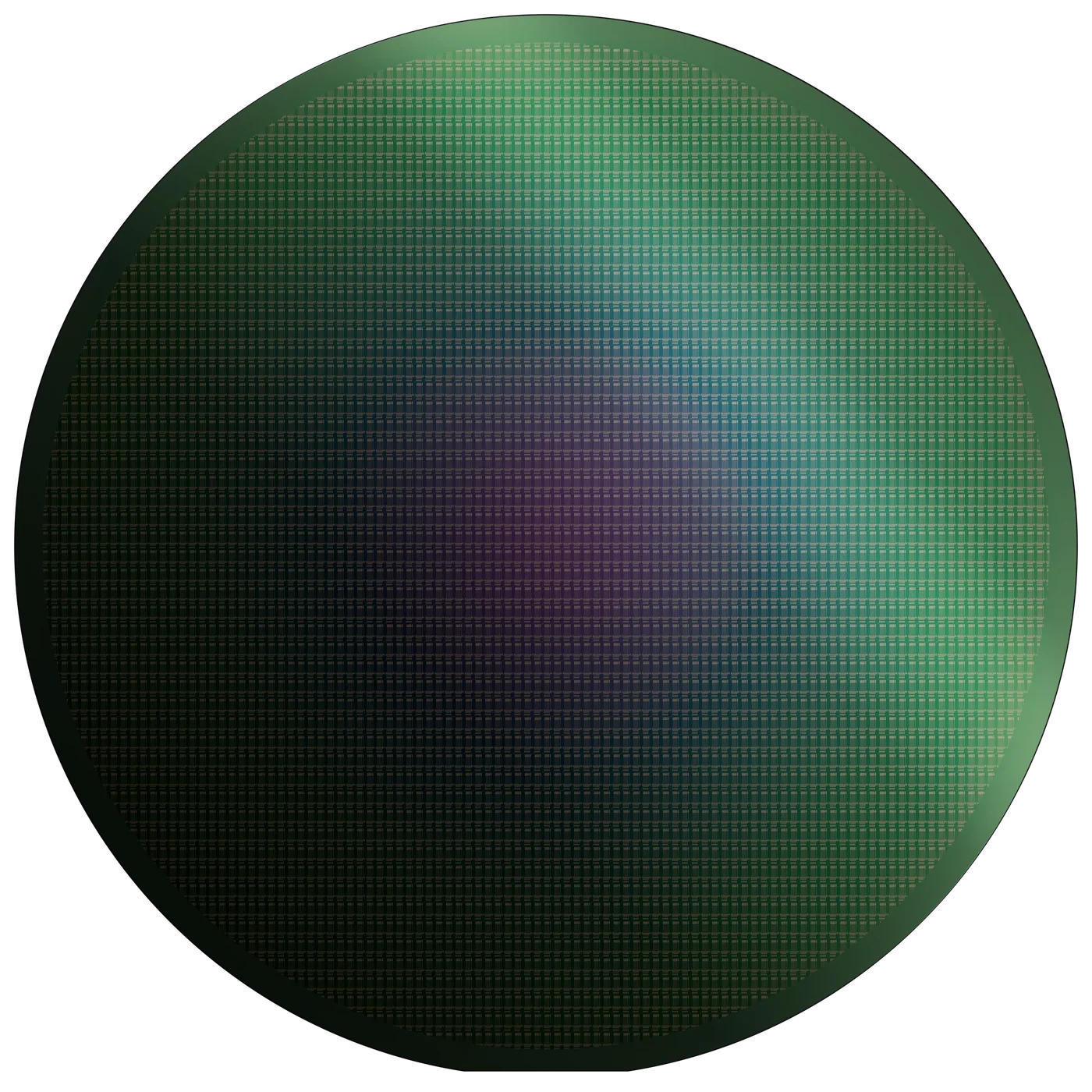
GaAs and InP wafers | Maryland, USA
The wafer
comes home
Every radar, satellite link and AI optical transceiver starts on a compound semiconductor wafer. We are building the first commercial-scale U.S. plant to make them.
Four elements. One American line.
The line
Element to epiwafer, under one roof

01Feedstock
U.S. gallium and indium from domestic suppliers, so the chain starts on American soil.
02Refining
Gallium and arsenic to 7N on site, with every lot measured for the impurities that matter.
03Synthesis
Polycrystalline GaAs and InP charges with controlled stoichiometry.
04Crystal growth
Vertical gradient freeze: a shallow thermal gradient, low stress, low dislocation density.
05Slicing and polishing
Multi-wire sawing, lapping and two-stage CMP to an epi-ready surface, with a roughness target below 0.2 nm Ra.
06Epitaxy
Device layers grown on our own wafers, MBE first with MOCVD for volume.
The wafers
Full specificationsEPD < 5×10³ρ > 10⁷ Ω·cmRF, radar, 5GSi-doped n-type GaAs150 mm
EPD < 500n 0.5–5×10¹⁸VCSELs, lasersS-doped n-type InP100 mm
EPD < 500n 1–8×10¹⁸Lasers, PICsFe-doped semi-insulating InP100 mm
EPD < 5×10³ρ > 10⁷ Ω·cmHEMT, DHBTUndoped InP100 mm
EPD On requestn 10¹⁵–10¹⁶Research, epitaxy
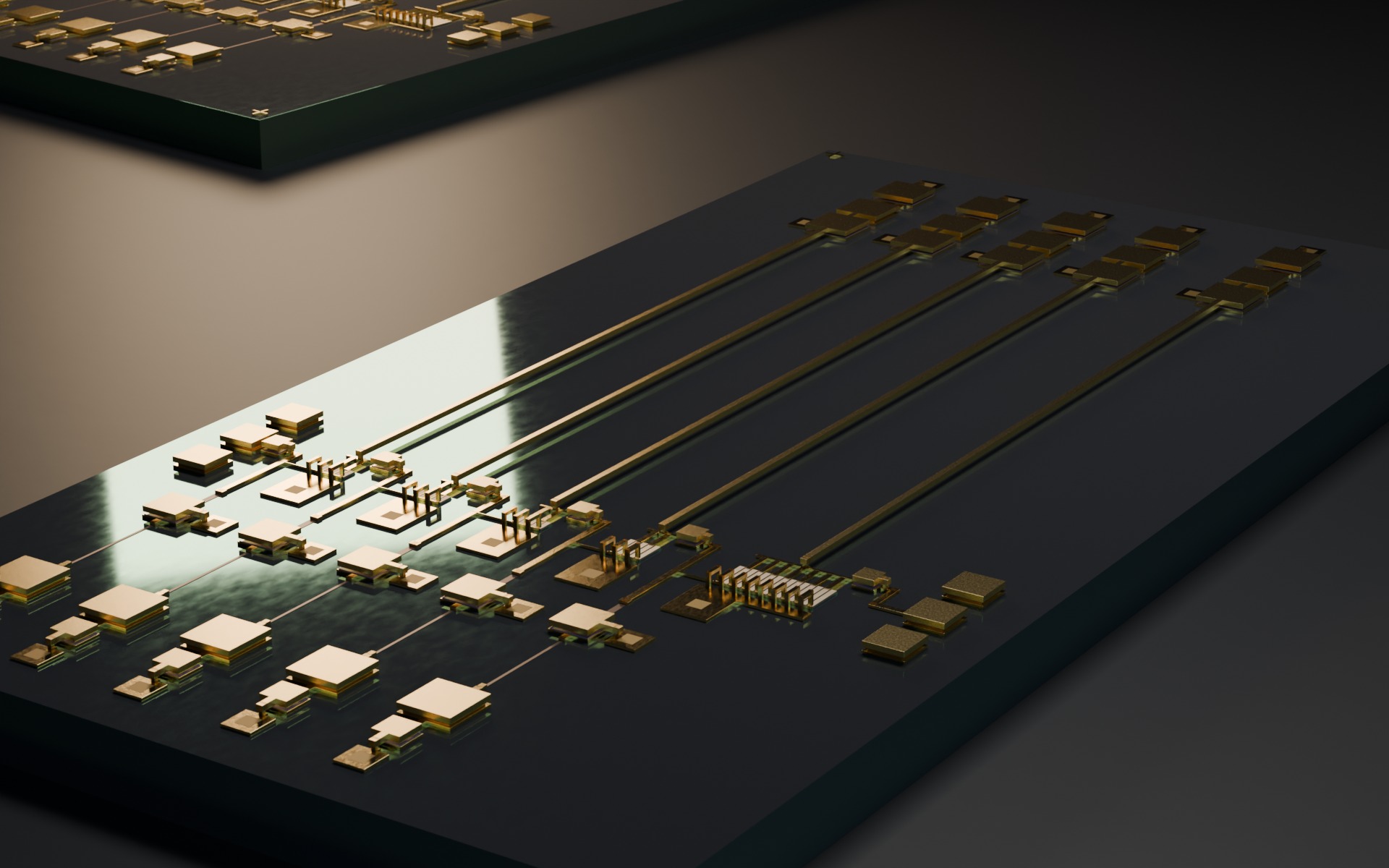
No U.S. plant grows these crystals today
China produces about 99% of the world’s primary gallium. The wafers beneath American defense and data-center chips are grown abroad, from imported elements.
Source: USGS Mineral Commodity Summaries 2026