Technology
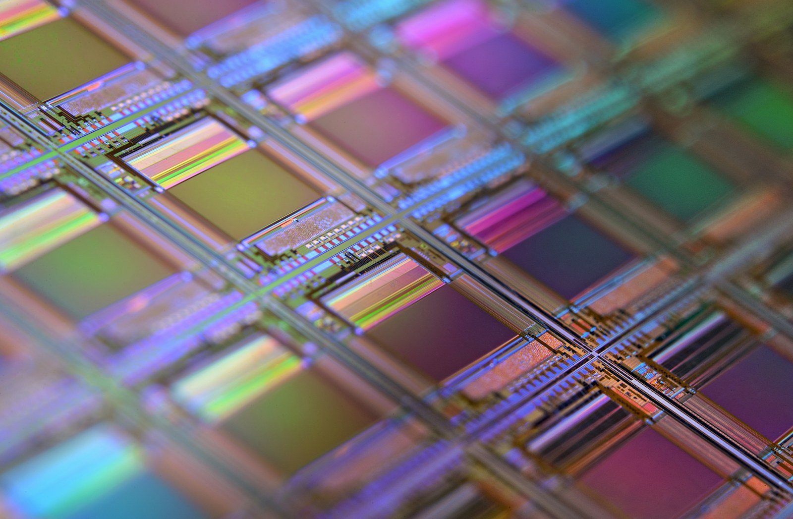
Patterned wafer, macro. Photo: Laura Ockel on Unsplash.
01
Feedstock
U.S. gallium and indium from domestic suppliers, so the chain starts on American soil.
02
Refining
Gallium and arsenic to 7N on site, with every lot measured for the impurities that matter.
03
Synthesis
Polycrystalline GaAs and InP charges with controlled stoichiometry.
04
Crystal growth
Vertical gradient freeze: a shallow thermal gradient, low stress, low dislocation density.
05
Slicing and polishing
Multi-wire sawing, lapping and two-stage CMP to an epi-ready surface, with a roughness target below 0.2 nm Ra.
06
Epitaxy
Device layers grown on our own wafers, MBE first with MOCVD for volume.
Services
Epiwafers
Buy a substrate or a finished epiwafer from one U.S. source.
Finishing and tolling
Lapping, CMP and epi-ready cleaning for allied crystal growers.
Reclaim
Recovery of gallium, arsenic and indium from III-V scrap.
High-purity elements
Merchant supply of refined 7N gallium and 7N arsenic.